A Novel of Solution-Processed High-Efficiency ETL SnO2 /PEI for enhanced Inverted OLED Performance
- 1. College of Physics and Electronic Engineering, Xingtai University, China
- 2. School of Chemical Engineering and Biotechnology, Xingtai University, China
ABSTRACT
Tin oxide (SnO2) has been extensive researched as an electron-transport layer (ETL) in inverted organic light emitting devices (OLEDs) because of its outstanding advantages in many aspects. However, there are defect sites for nonradiative recombination, which have limited its widespread application as ETLs in the SnO2 -based OLEDs. Herein, a novel approach utilizing Polyethyleneimine (PEI) for modifying SnO2 is introduced. OLEDs were fabricated with the structure of ITO/ SnO2 / PEI/ PVK: Alq3/ NPB/ MoO3/ Al. The atomic force microscopy (AFM), photoluminescence (PL), Time-Resolved Fluorescence Transient Lifetime (TRPL) and current density-voltage-luminescence of the OLEDs were characterized, then the dependence of SnO2 and PEI thickness on device characteristics was investigated. It revealed that this modification serves dual purposes of roughness reduction and surface-defect passivation, can inhibit the leakage current of OLEDs and avoid the quenching of excitons. OLEDs with PEI-modified SnO2 (SnO2 /PEI) ETL exhibit a remarkable current efficiency (CE) of 3.15 cd/A, which significantly exceeds that (0.85 cd/A) achieved with bare SnO2 -based OLEDs, along with effectually reducing the turn-on voltage from 4.5 to 3.5 V. This study confirms the efficacy of PEI for efficient OLEDs, paving the way for SnO2 applications.
KEYWORDS
• Solution-Processed
• ETL;
• SnO2
• Inverted OLED
CITATION
Gao S, Guo H, Guo G, Li Y (2025) A Novel of Solution-Processed High-Efficiency ETL SnO2 /PEI for enhanced Inverted OLED Performance. J Phys Appl and Mech 2(1): 1007.
INTRODUCTION
SnO2 can be utilized in a large number of applications and been reviewed by several researchers due to its high transparency, low cost, low toxicity, widespread availability high stability and great flexibility in structure [1-4]. In particular, SnO2 as an n-type oxide has excellent electron mobility [5]. Significant advantages of the SnO2 as mentioned above make SnO2 an efficient and well-explored electron transport material in photoelectronic device. As a matter of fact, it has been widely utilized as an ETL material for various solar cells with remarkable results [6-8]. In the same way, transparent materials are more favourable for OLED devices, in particular, SnO2 , as electron transporting material, is a good choice of material for ETL in bottomemission inverted OLEDs. ZnO, which is similar to SnO2 , has also been widely studied as an electron transport layer [9,10], but SnO2 has been confirmed to have more advantages in bottom-emission inverted OLEDs. Park et al. compared the properties of SnO2 as the ETM with those of ZnO by transmission electron microscopy (TEM) and atomic force microscopy (AFM) images, indicating that SnO2 NPs have a smoother surface, which allows better layer-by-layer connection [11].
In addition, the carrier concentration of ZnO is more than two times higher than that of SnO2 , which will cause excessive electron injection, leading to imbalance with holes. SnO2 NPs exhibit lower carrier concentration but the same electron mobility, indicating more suitable to result in improved OLED device performance [6]. Lee et al. applied SnO2 NPs as an interface layer between the ITO cathode and the ETL in an inverted bottom-emission OLED device. It was helpful to form a ladder-like energy alignment from ITO to the emitter to facilitate the electron injection [12]. Therefore, we introduce SnO2 as an ETL for research. However, Trost S and Abel B et al., reported that abundance of oxygen vacancies originating from the nanoparticle structure of SnO2 and numerous exposed hydroxyl groups on the surface, which are ormed by adsorbed oxygen from the air, act as defect sites for nonradiative recombination. This leads to reduced conductivity of SnO2 films and adversely affects the performance of SnO2 -based devices [13,14]. In this regard, Kim D et al., incorporated synthesized u-PEIs into the SnO2 layer of OSC devices to effectively passivate the surface defects on SnO2 [7]. Shen P et al., study the SnO2 /PFN bilayer structure of inverted PSCs and the corresponding PCE is dramatically improved compared to the device with SnO2 -only [15]. In this work, we reported PEI-modified SnO2 (SnO2 /PEI) ETL and their application in bottom inverted OLED based on PVK: Alq3 EML by solution-processed.
The PEI modification can significantly improve the device CE from 0.85 to 3.09 cd /A. The main effect of PEI modification is associated with surface roughness and defect passivation of SnO2 , which has been proven by atomic force microscopy (AFM) and time-resolved fluorescence transient lifetime (TRPL). The modification reduces the leakage current and exciton quenching, improving the exciton utilization. The EL performance of the devices with SnO2 /PEI is better than that of the SnO2 reference device.
EXPERIMENTAL
The OLEDs with the structure of ITO/SnO2 /PEI/EML/ NPB/MoO3/Al were fabricated, and the schematic diagram of the structure is shown in the illustration in Figure 1, in which SnO2colloidal solution mixed with ammonia was spin-coated at 4000 rpm for 30 s and annealed at 170? for 30 min in the surrounding environment to obtain the ETL. and then transfer the substrate into the argon atmosphere glove box and spin-coated with PEI and EML. PEI dissolve in alcohol were spin-coated on ETL at 3000 rpm for 40 s and annealed at 130 ? for 20 min. The molecular structure of PEI is shown in Figure 1.
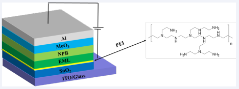
Figure 1 The structure of inverted OLED and the molecular structure of PEI polymer
The polymer PVK doped with Alq3 was used as the emitting layer (EML), which the weight ratio of [6:4 mg/mg] in 1 mL DMF (N, N- dimethylformamide) solution were spin- coated on PEI at 2000 rpm for 30 s and annealed at 110? for 15 min. NPB and MoO3/Al were used as the hole transport layer (HTL) and modified anode, respectively. NPB, MoO3 and Al were sequentially deposited onto the above substrate. The thermal evaporation process was carried out in an Edwards Auto-500 thermal evaporation system at a pressure of 1×10⁻⁵ Pa, and an in-situ quartz crystal was used to monitor the thickness of the vacuum depositions. The evaporation rates were 0.2 nm/s, 0.07 nm/s and 1.0 nm/s for the NPB, MoO3 and Al, respectively. All devices were prepared on pre-patterned indium tin oxide (ITO) coated glass substrate with a sheet resistance of 15 Ω/sq. The substrates were treated in an ultraviolet- ozone chamber for 20 min after the following cleaning procedure: ultrasonically cleaned with detergent, acetone, ethanol and deionized water.
RESULTS AND DISCUSSION
The electron transport material SnO2 has been demonstrated to be highly efficient, cross-linkable ETL in inverted OLEDs and organic solar cells [16-18]. We first investigate the current density (J)–bias (V)–luminance (L) characteristics of OLED devices with an inverted structure as follows. Device A: ITO/SnO2 (8 wt.%)/EML/NPB (30 nm)/ MoO3(5 nm)/Al (120 nm) Device B: ITO/SnO2 (8 wt.%)/PEI (0.15 wt.%)/EML/ NPB (30 nm)/MoO3(5 nm)/Al (120 nm), As can be seen from Figure 2,
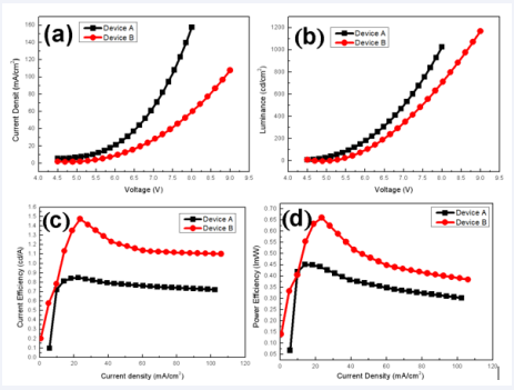
Figure 2 The EL performances of Device A and B The current density-voltage curves;(b) The luminance-voltage curves; (c) The current efficiency-current density characteristics; (d) The power efficiency-current density characters
compared with Device A, Device B reduces the current density obviously, and the turn-on voltage changed negligibly. It is believed that the PEI layer are responsible for device performance enhancement. In Figure 2 (c) and (d), with single SnO2 ETL, Device A shows poor device efficiency, the maximum CE is only 0.85 cd/A, and the maximum power efficiency (PE) is 0.45 lm/w. With PEI modified ETL, Device B improves the CE and PE to 1.47 cd/A and 0.66 lm/w. To understand why the PEI modification improves the performance of Device B, we first investigated the morphology of SnO2 and SnO2 /PEI thin films. The AFM images are shown in Figure 3. The root mean square (Rq) values of the roughness for the ITO/SnO2 (8 wt.%) and ITO/SnO2 (8 wt.%)/PEI (0.15 wt.%) samples are 1.31 nm and 0.34 nm, respectively. Thus, PEI covered and reduced the surface.
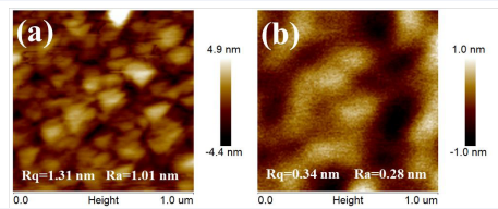
Figure 3 The AFM image of thin films spin coated by 8 wt.% SnO2 solution; (b) The AFM image of spin-coated with 0.15 wt.% PEI thin film on SnO2 layer.
Roughness of the SnO2 layer. Therefore, it should be due to PEI layer modified the surface roughness of SnO2 layer, effectively inhibiting the generation of leakage current and improving the luminescence performance of the device [19]. In order to further reveal the reasons of PEI layer improves the luminescence performance of Device B, the photoluminescence (PL) spectrum and time-resolved fluorescence transient lifetime (TRPL) measurement were carried out as a tool to elucidate the exciton lifetime at the interface of ETL/EML based on the ITO/SnO2 /EML and ITO/SnO2 /PEI/EML structures. PL spectrum of the two samples with excitation wavelengths of 410 nm are shown in Figure 4(a). It is observed that the emission spectrum of their peaks are approximately identical. It suggests that the addition of PEI layer does not affect the transfer state of excitons in the EML [20]. Figure 4(b) shows the room temperature PL decay curves of the studied samples measured at the PL peak emission energy, and each decay curve can be well fitted by a double exponential function expressed as: [1]
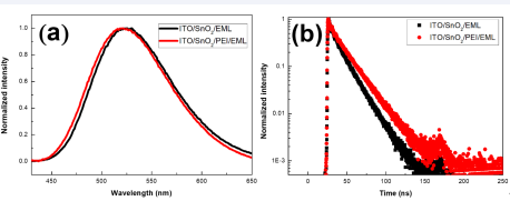
Figure 4 PL spectrum and (b) TRPL decay curves measured for SnO2 /EML and SnO2 /PEI/EML
Y = A1 exp(-t /t1 ) + A2 exp(-t /t 2 ) + y0
Where A1 (A2) representstheamplitudeofthe fast decay (slow decay) component at t = 0. τ1 and τ2 represent the decay time of slow and fast components, which correspond to the radiative and non-radiative recombination processes of excitons respectively [21,22]. It is well known that the quantum yield of the film is in direct proportion to the average fluorescence lifetime [23].We can get the result that the excitons average lifetime of the ITO/SnO2 / PEI/EML (13.6 ns) is better than the ITO/SnO2 /EML (10.7 ns) case, indicating that the device with SnO2 /PEI as ETL has the potential to produce a high EL performance [24], which may be due to the isolation and passivation of PEI and avoiding the exciton quenching by SnO2 surface defects [13,14]. Analyses above proved that SnO2 /PEI interface modification is an effective way to improve the device performance. In this way, the utilization rate of excitons in light-emitting devices can be improved, thus improving the performance of light-emitting devices. It’s known from above characteristics that SnO2 /PEI can effectively improve the luminescence performance of devices. Next, the dependence of SnO2 and PEI thickness on device characteristics was then investigated. The light emitting device structure used in this experiment is ITO/SnO2 /PEI/ EML/NPB (30 nm)/MoO3 (5 nm)/Al (120 nm). Firstly, the thickness of SnO2 layer is optimized. In this experiment, the solution concentration used for spin coating PEI layer is 0.15 wt.%, and the solution concentration of SnO2 is set to 2, 3, 4, and 5 wt.%, respectively. The corresponding devices are named Device C-F in turn. Figure 5 shows the EL performance of device C-F. It can be seen that the current density, luminance and current efficiency of these devices have the same trend, which first increase and then decrease with the increase of SnO2 solution concentration.
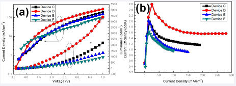
Figure 5 The EL performances of Device C-F (a) The current density-voltage-luminance curves;(b) The current efficiency-current density characteristics
The turn-on voltage (at 1cd/m2) of these devices were 3.7, 3.6, 3.7 and 3.8 V, respectively. It was obvious that the Device D presented a maximum luminance of 4401 cd/m2 at 7 V, a maximum CE of 2.60 cd/A at 15.7 mA/cm2. That is to say, the optimal structure of the device was achieved when the concentration of SnO2 solution was 3 wt.%, which was consistent with the statements in relevant literatures [12]. It may be attributed to the fact that the thickness of SnO2 film continues to increase as the increase of the SnO2 solution concentration, which enhances the film- forming property and helpful to form a ladder-like energy alignment from ITO to the EML [12], effectively reduces the occurrence of leakage current and facilitate the electron injection. However, when the thickness of SnO2 film is too large, the transmission resistance increases, causing the device performance deteriorates. The dependence of device characteristics on PEI concentration was then investigated as the structure of ITO/SnO2 /PEI/EML/NPB (30 nm)/MoO3(5 nm)/Al (120 nm). The concentration of PEI is varied to 0.05, 0.10, 0.15 or 0.20 wt.%, and the SnO2 solution concentration was fixed at 3 wt.%. The devices corresponding to different PEI concentrations are named as Device G-J in turn, in which the structure of Device I is exactly the same as that of Device D in the previous group experiments, and the EL characteristics curves of Device G-J are shown in Figure 6.
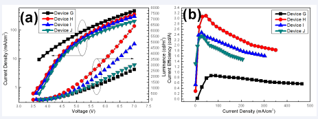
Figure 6 The EL performances of Device G-J a) The current density-voltage-luminance curves; (b) The current efficiency-current density characteristics.
It can be clearly seen from Figure 6 that the current density of these OLEDs gradually decrease with the increase of PEI concentration. The luminance, current efficiency and power efficiency of these devices have the same trend, which first increase and then decrease with the increase of PEI solution concentration. It is considered that the PEI layer are too thin to completely cover the surface roughness at the solution concentration of 0.05 wt.% [19]. The result is that device H exhibited the lowest turn-on voltage (at 1 cd/m2) of 3.5 V, maximum luminance of 6395 cd/m2 at 7V and maximum current efficiency of 3.15 cd/A at 42.0 mA/cm2. It is considered that the PEI can modify and passivate SnO surface defect to improve the performance of OLED devices [15]. However, when the PEI solution concentration exceeds 0.1 wt.%, the device performance gradually decreases, because PEI is an insulator, and the conductivity is poor [25] (Table 1).
Table 1: Summary of EL performances of devices in this work.
|
Device |
ETL: ITO/SnO2/PEI/ |
Turn-on voltage (V) |
Max. L (cd/m2) |
Max. CE (cd/A) |
|
|
SnO2 (wt.%) |
PEI (wt.%) |
||||
|
A |
8 |
-- |
4.5 |
1023 |
0.85 |
|
B |
8 |
0.15 |
4.5 |
1168 |
1.47 |
|
C |
2 |
0.15 |
3.7 |
2197 |
1.99 |
|
D |
3 |
0.15 |
3.6 |
4401 |
2.60 |
|
E |
4 |
0.15 |
3.7 |
1347 |
2.07 |
|
F |
5 |
0.15 |
3.8 |
969 |
1.66 |
|
G |
3 |
0.05 |
3.7 |
2631 |
0.89 |
|
H |
3 |
0.10 |
3.5 |
6395 |
3.15 |
|
I |
3 |
0.15 |
3.6 |
4846 |
2.61 |
|
G |
3 |
0.20 |
3.7 |
3043 |
2.37 |
CONCLUSION
In summary, a novel solution-prossed SnO2 /PEI modified ETL has been developed for a inverted OLED. We found that the composite ETL in inverted OLED provided two main advantages: 1) reducing the surface roughness of SnO2 to inhibit the leakage current and 2) passivating the surface defects on SnO2 to avoid the quenching of excitons to improve the EL performance of the device. Compared to SnO2 single ETL device (Device A), the optimized SnO2 / PEI modified ETL device (Device H) reaches the maximum luminance 6395 cd/m2, increased by 5.3 time, enhances the CE from 0.85 to 3.15 cd /A, increased by 2.7 time, and effectually reduces the turn-on voltage from 4.5 to 3.5 V, demonstrating better electron transport and injection. Therefore, finding functional material with the ability to modified the SnO2 surface is crucial for the development of efficient SnO2 -based devices.
REFERENCES
- Liu Y, Jiao Y, Zhang Z, Qu F, Umar A, Wu X. Hierarchical SnO2 Nanostructures Made of Intermingled Ultrathin Nanosheets for,Environmental Remediation, Smart Gas Sensor, andSupercapacitor,Applications. ACS. 2014; 6: 2174-2184.
- Pusawale SN, Deshmukh PR, Lokhande CD. Chemical synthesis of nanocrystalline SnO2 thin films for supercapacitor application. Appl Surface Sci. 2011; 256: 9498-9502.
- Wang C, Du G, Ståhl K, Huang H, Zhong Y, Jiang JZ. Ultrathin SnO2 Nanosheets: Oriented Attachment Mechanism, Nonstoichiometric Defects, and Enhanced Lithium-Ion Battery Performances. The J Phys Chem C. 2012; 116: 4000-4011.
- Wang H, Rogach AL. Hierarchical SnO2 Nanostructures: Recent Advances in Design, Synthesis, and Applications. Chem Mat. 2013; 26: 123-133.
- Zhang Y, Hu Z, Liang Y, Yang Y, An N, Li Z, et al. Growth of 3D SnO2 nanosheets on carbon cloth as a binder-free electrode for supercapacitors. J Mat Chem. 2015; 3: 15057-15067.
- Dalapati GK, Sharma H, Guchhait A, Chakrabarty N, Bamola P, Liu Q, et al. Tin oxide for optoelectronic, photovoltaic and energy storage devices: a review. J Mat Chem. 2021; 9: 16621-16684.
- Kim D, Lee S, Oh CM, Hwang IW, Yoon C, Kim C, et al. Hong, Bifunctional Urea–Polyethyleneimine-Mediated Surface Engineering in SnO2 Electron-Transport Layer for Efficient and Stable Organic Solar Cells. Solar RRL. 2024; 8.
- Yoo JJ, Seo G, Chua MR, Park TG, Lu Y, Rotermund F, et al. Efficient perovskite solar cells via improved carrier management. Nature. 2021; 590: 587-593.
- Musavi H, Fadavieslam MR. Improving organic light-emitting diode,performance with ZnO nanoparticles. J Mat Sci. 2017; 28: 7797-7801.
- Park S, Suh M, Kim K, Kim M, Cho H, Shin H, et al. Effect of spatial molecular configuration of ZnO/ polyethylenimine hybrid electron injection materials on OLEDs performance. Organic Electronics. 2019; 75: 105427.
- Park M, Song J, An M, Lim J, Lee C, Roh J, et al. Colloidal quantum dot light-emitting diodes employing solution-processable tin dioxide nanoparticles in an electron transport layer. RSC Adv. 2020; 10: 8261-8265.
- Lee H, Kang CM, Park M, Kwak J, Lee C. Improved Efficiency of Inverted Organic Light-Emitting Diodes Using Tin Dioxide Nanoparticles as an Electron Injection Layer. ACS. 2013; 5: 1977-1981.
- Abel B, Buck U, Sobolewski AL, Domcke W. On the nature and signatures of the solvated electron in water. Phys Chem Chem Phys. 2012; 14: 22-34.
- Trost S, Behrendt A, Becker T, Polywka A, Görrn P, Riedl T. Tin Oxide (SnOx) as Universal “Light-Soaking” Free Electron Extraction Material for Organic Solar Cells. Adv Energy Mat. 2015; 5.
- Shen P, Yao M, Wang G, Mi R, Guo W, Bai Y, et al. High-efficiency polymer solar cells with low temperature solution-processed SnO2/ PFN as a dual-function electron transporting layer. J Mat Chem A. 2018; 6: 17401-17408.
- Earmme T, Jenekhe SA. Solution-Processed, Alkali Metal-Salt-Doped, Electron-Transport Layers for High-Performance Phosphorescent Organic Light-Emitting Diodes. Adv Functional Mat. 2012; 22: 5126-5136.
- Kwon JH, Lee JY. High efficiency and long lifetime in organic light- emitting diodes using bilayer electron injection structure. Synthetic Metals. 2009; 159: 1292-1294.
- Liu J, Wu X, Shi X, Wang J, Min Z, Wang Y, et al. Highly Efficient and Stable Electron Injection Layer for Inverted Organic Light-Emitting Diodes. ACS. 2015; 7: 6438-6443.
- Kurosawa Y, Murakami T, Takahashi T, Suzuri Y. Coverage Performance of PEDOT: PSS Against Particles on a Substrate for OLEDs. Adv Mat Interfaces. 2022; 10: 2201695
- Chen D, Wang Z, Wang D, Wu YC, Lo CC, Lien A, et al. Efficient exciplex organic light-emitting diodes with a bipolar acceptor. Organic Electronics. 2015; 25: 79-84.
- de Mello Donegá C, Bode M, Meijerink A. Size- and temperature- dependence of exciton lifetimes in CdSe quantum dots. Phys Rev. 2006; 74.
- Smida A, Zaaboub Z, Mohamed H, Hassen M, Laatar F, Maaref H, et al. Photoluminescence behavior in the synthesized CdSe thin films deposited on ITO substrates. J Luminescence. 2018; 194: 686-691.
- Ravi Kishore VVN, Narasimhan KL, Periasamy N. On the radiative lifetime, quantum yield and fluorescence decay of Alq in thin filmsElectronic supplementary information (ESI) available: Experimental data. Phy Chem Chem Phy. 2003; 5: 1386-1391.
- Li Y, Gao S, Zhang N, Huang X, Tian J, Xu F, et al. Solution-processable, high luminance deep-blue organic light emitting devices based on novel naphthalene bridged bis-triphenylamine derivatives. J Mat Chem. 2019; 7: 2686-2698.
- Hu L, Zhao N, Jiang X, Jiang Y, Qin F, Sun L, et al. Sn–N/Sn–O interaction improving electron collection in non-fullerene organic solar cells. J Mat Chem. 2020; 8: 12218-12223.